


 Damage
  Loss
Loss  Theft
Theft 


CCD vs. CMOS Sensors
CCD Sensors

CMOS Sensors
The ongoing discussion surrounding the strengths of CCD versus CMOS image sensors has lasted for decades — and there is still no simple, one-size-fits-all answer. That is because the landscape is always shifting. Technology advances, markets evolve, and commercial realities change what is feasible at any given time. Different imaging tasks have unique needs, and some are best addressed by CMOS, while others still favor CCD. This article aims to shed light on the nuances of each sensor type, uncover some of the lesser-discussed technical trade-offs, and factor in the real-world cost implications that influence buying decisions.
In the Beginning...
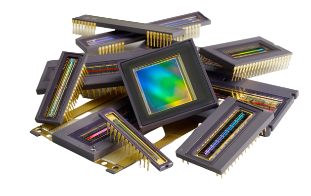
CCD (charge coupled device) and CMOS (complementary metal oxide semiconductor) image sensors represent two fundamentally different approaches to converting light into a digital image. Each possesses a distinct set of advantages and drawbacks depending on the specific application at hand.
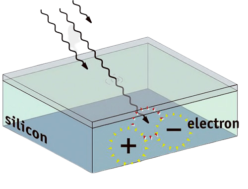
At their core, both sensor types turn incoming light into an electrical charge that gets processed into a usable electronic signal. In a CCD sensor, the charge from every pixel is funneled through a very small number of output nodes — sometimes only one — where it is converted into voltage, buffered, and transmitted off-chip as an analog signal. Because of this design, the entire pixel area can be dedicated to gathering light, resulting in high output uniformity, which is a major contributor to overall image quality.
In a CMOS sensor, each individual pixel contains its own charge-to-voltage converter, along with additional circuitry such as amplifiers, noise-correction modules, and digitization components. The chip produces digital output directly. This added complexity does reduce the pixel's light-gathering area and introduces some uniformity challenges, but the massively parallel nature of the architecture enables remarkably high-speed data throughput.
Both CCD and CMOS imagers were originally developed in the late 1960s and 1970s. For years, CCD sensors dominated the market because they produced noticeably superior images given the manufacturing capabilities of the time. CMOS sensors demanded finer lithographic processes and tighter uniformity than early silicon foundries could reliably deliver. It was not until the 1990s that fabrication technology advanced enough to make CMOS a serious contender once again.
The renewed enthusiasm for CMOS was largely driven by expectations of lower power consumption, the ability to integrate the full camera system onto a single chip, and reduced manufacturing costs by leveraging existing logic and memory fabrication lines. While achieving these goals alongside excellent image quality took considerably more time and investment than initially predicted, CMOS imagers have since matured into a mainstream, widely adopted technology alongside CCD.
High Volume Imagers for Consumer Applications
Riding the wave of lower power consumption and compact integration, CMOS engineers focused their attention on the mobile phone market — the single largest application for image sensors worldwide. The staggering level of investment that poured into developing and perfecting CMOS sensors for smartphones led to dramatic improvements in quality, even as pixel sizes continued to shrink. As a result, for high-volume consumer applications and line scan imaging, CMOS sensors now outperform CCDs on nearly every performance metric.

Imagers for Machine Vision
In the world of machine vision, area and line scan imagers benefited enormously from the momentum of smartphone sensor development. The massive investment in mobile CMOS technology effectively paved the way for CMOS to displace CCD in most machine vision and line scan applications. For the majority of these use cases, CCD technology is now considered a thing of the past.
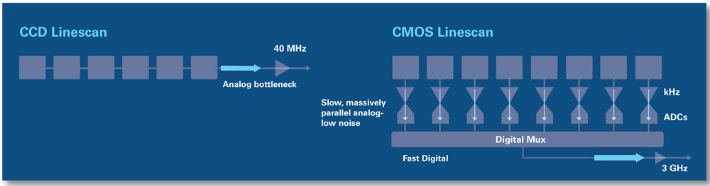
The speed and noise advantages of CMOS in machine vision deserve a closer look. For these applications, speed and noise levels are the critical parameters. The way each sensor type converts the signal charge to analog, and then to digital, makes all the difference. In CMOS area and line scan imagers, the front-end data path operates in a massively parallel fashion. Each amplifier handles only a modest amount of bandwidth. By the time data reaches the bottleneck — typically the interface between the chip and external circuitry — it is already in the digital domain.
High-speed CCDs, on the other hand, use multiple fast output channels that are not as massively parallel. Each CCD amplifier must handle greater bandwidth, which inherently introduces more noise. As a consequence, high-speed CMOS sensors can be engineered for significantly lower noise levels than their high-speed CCD counterparts.
That said, there are noteworthy exceptions to this general rule.
Near Infrared Imagers
Capturing images in the near infrared range (700 to 1000nm) requires sensors with a thicker photon absorption layer. This is because infrared photons penetrate deeper into silicon than visible light photons do.
Most CMOS fabrication processes are optimized for high-volume visible-light applications, making them inherently less sensitive in the NIR spectrum. In fact, many are intentionally designed to minimize NIR response. Increasing the substrate or epitaxial layer thickness to boost infrared sensitivity can compromise the sensor's spatial resolution, and the associated changes in voltage and doping levels can disrupt the operation of the CMOS analog and digital circuits.

CCDs, however, can be manufactured with much thicker epitaxial layers while still maintaining sharp spatial resolution. Some specialized near infrared CCDs feature epi layers exceeding 100 microns — far more than the 5 to 10 microns found in standard CMOS sensors. The pixel biasing and epi concentration adjustments needed for thicker layers are much simpler to manage in the CCD architecture.
The takeaway: CCDs specifically engineered for near infrared sensitivity deliver substantially higher performance than their CMOS equivalents in this spectral range.
Ultraviolet Imagers
Because ultraviolet photons are absorbed extremely close to the silicon surface, UV sensors must avoid having polysilicon, thick nitride, or heavy oxide layers that would block UV photon absorption. Modern UV sensors are therefore backside thinned, with only a very thin anti-reflective coating applied to the imaging surface.
While backside thinning has become commonplace in consumer mobile imagers, achieving stable UV response is an entirely different matter. Regardless of whether the sensor is CCD or CMOS, the imaging surface must undergo specialized treatments for reliable UV performance. Many backside-thinned imagers designed for visible light use thick oxide layers that can discolor and degrade under prolonged UV exposure. Others use heavily doped boron passivation layers that extend too deep into the silicon, causing UV-generated electrons to recombine before they can be captured.
UV capability and backside thinning are achievable in all line scan sensors, but not every area imager qualifies. No global shutter CCD can be fully backside thinned. CMOS area imagers with rolling shutters can be, though conventional global shutter CMOS designs face their own challenges when thinned — storage nodes may become vulnerable to incident light, and shielding parts of the pixel on a thinned substrate without severely reducing the fill factor is extremely difficult. Some alternative global shutter CMOS designs avoid light-sensitive storage nodes entirely, but they come with trade-offs including higher noise, reduced full well capacity, or rolling shutter behavior.
Time Delay and Integration Imagers
Beyond standard area and line scan sensors, there is a specialized category called time delay and integration (TDI) imagers. Widely used in machine vision and remote sensing, TDI sensors function similarly to line scan imagers but employ many lines — often hundreds — instead of just one. As the subject being imaged passes each successive line, that line captures its own snapshot. The multiple snapshots are then combined to produce a stronger composite signal, making TDI imagers especially valuable when dealing with very faint signals.

CCD-based TDI sensors combine signal charges directly, and the summing process can be carried out with virtually zero added noise. CMOS TDIs can sum either voltages or charges, but voltage-domain summing is inherently noisier. As the number of rows increases, the accumulated noise in a CMOS voltage-domain TDI eventually undermines its ability to compete with the noiseless charge summation of a CCD TDI.
The trade-off comes down to speed versus sensitivity. CCD TDI offers outstanding sensitivity but hits a speed ceiling. CMOS has the speed advantage, yet charge-domain CMOS TDI designs are more complex and expensive to develop and build. For applications with fewer rows of summation, voltage-domain CMOS TDI delivers excellent cost-effective performance. But for the most demanding scenarios — maximum speed at minimum light — charge-domain CMOS TDI achieves the highest overall performance.
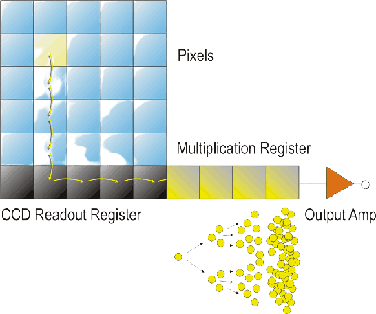
Electron Multiplication
Electron multiplication CCDs (EMCCDs) are a specialized type of CCD equipped with a multiplication register that amplifies the signal charge while keeping multiplication-related noise tightly controlled. The result is a meaningful boost in signal-to-noise ratio (SNR). In scenarios where the target signal is so faint that it barely rises above the sensor's noise floor, EMCCDs can reveal details that would otherwise go undetected.
EMCCDs show their greatest advantage over CMOS when the imaging task does not demand high frame rates. Operating at higher speeds increases read noise in CCDs, and once that happens, the SNR benefit of the multiplication register diminishes. At high speeds, the gap between an EMCCD and a modern scientific CMOS imager designed for very low read noise may not be significant. Additionally, high-speed EMCCDs consume considerably more power than conventional sensors.
It is also worth noting that even a low-noise CMOS sensor may lack the NIR, UV, or TDI-related advantages of a CCD. Because the incoming signal in those scenarios can be inherently much weaker, even when read noise levels are comparable, an EMCCD-based solution may ultimately deliver better overall performance.
Cost Considerations
Up to this point, we have examined the performance differences between CCD and CMOS sensors. But it would be unrealistic to think that real-world decisions are based purely on performance. For most decision-makers, what matters most is value — the level of performance you get for the price you pay. The cost equation can be nuanced, but several key principles stand out.
Leverage is king. Off-the-shelf sensors will always cost far less than custom-designed ones, regardless of whether they are CCD or CMOS. When customization is unavoidable, building a custom CCD is typically cheaper than developing a custom CMOS sensor, since CMOS designs require more expensive deep submicron masks and significantly more on-chip circuitry. In some cases, even when a custom CMOS imager would technically outperform a CCD, the value proposition still favors the CCD.
Volume matters. While the upfront development cost of a new CMOS imager tends to be higher, CMOS sensors that achieve high production volumes benefit from greater economies of scale, driving down the per-unit cost. At scale, a low per-unit cost can far outweigh a higher initial development investment.
Supply security counts. Being left with a product built around a sensor that has been discontinued is extremely costly. Despite potentially better specs on paper, choosing a supplier with the strongest long-term ability to produce the imager — CCD or CMOS — may be the wiser business decision.
Conclusion
Selecting the right image sensor for a given task has never been straightforward. Every application comes with its own unique requirements and constraints that influence both performance and pricing. Given these intricacies, making a blanket statement about CCD versus CMOS that holds true across all use cases is simply not possible.
In summary, CMOS area and line scan sensors outperform CCDs across the majority of visible imaging applications. CCD-based TDI sensors remain superior for high-speed, low-light-level tasks, outpacing CMOS TDIs. The need for near infrared sensitivity can make CCDs the clear winner for certain area and line scan uses. For ultraviolet imaging, the quality of the post-thinning surface treatment matters most, and global shutter requirements further narrow the options. Extremely low-noise demands add yet another layer of complexity, with CMOS generally still edging out CCDs at high readout speeds. And when it comes to the cost equation, the right choice between CCD and CMOS ultimately depends on leverage, production volume, and long-term supply security.
Featured Product
Experience CCD Imaging at Its Finest
Explore the legendary CCD sensor quality of the Leica M9 — a camera that defined an era of digital rangefinder photography.